|
|
|
|
News The Project Technology RoboSpatium Contribute Subject index Download Responses Games Gadgets Contact <<< Simple Communication Switching P-channel MOSFETs >>> N-channel MOSFETsThere is no Video about switching MOSFETs available, yet.Leave a comment, if you have ideas of what to show in that video (besides the things already mentioned on this page).OverviewIn this chapter you can read about:
Limits of switching loads with GPIO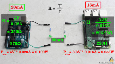
In the previous chapter we learned how to switch LEDs directly using GPIOs. The maximum switchable electrical power of a load is limited by the specifications of the General Purpose Input Output pins of the respective computer. An Arduino Uno and a Raspberry Pi can be seen in the photo. The former works with a logic voltage of 5V and can switch currents of up to 50mA directly on a GPIO. The resulting maximum power is 0.25W. The limit for the Raspberry Pi is 16mA at 3.3V logic level which is just 0.053W. As can be seen, the switchable power is rather small. In this chapter, I will therefore show, how the power to be switched can be amplified using MOSFETs. MOSFET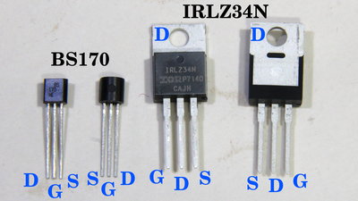
MOSFET stands for Metal Oxide Semiconductor Field Effect Transistor. Electrical signals can be amplified with this type of semiconductor device. MOSFETs are active devices having usually 3 terminals, which are called source, gate and drain. What pin leads internally to what connection can be found in the datasheet of the transistor. The connections are not standardized and swapping them will most likely lead to the destruction of the transistor! The resistance between source and drain can be varied depending on the gate voltage and this property can be used to amplify electrical signals. N-channel MOSFET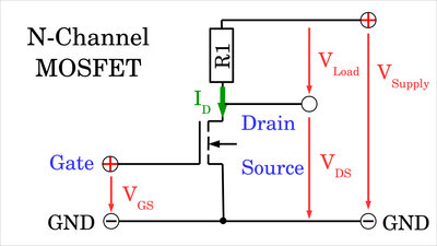
Let take a closer look at an N-channel MOSFET on a simple DC voltage source. The amplifier consists of two circuits, both of which are joined via the ground line (the negative terminal of your voltage source). The source pin of the MOSFET is also connected directly to ground. The input circuit consists only of a variable voltage source, with the positive terminal being connected to the gate pin. The output circuit consists of a constant DC voltage source, with the positive terminal leading via a load (here an ohmic resistor) to the drain pin of the transistor. 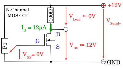
An experimental setup for examining the properties of a MOSFET can be seen here. As before, the drain pin in the output circuit is connected to the positive terminal of a +12V DC voltage source via a load resistor. The input circuit consists of a potentiometer, which is also connected to the +12V terminal of the voltage source and to ground on the other side. The wiper leads to the gate pin of the MOSFET. If this sliding contact is at the lower stop, the gate pin is connected directly to ground, so there is 0V between source and gate of the transistor. As written before, the resistance between source and drain depends on this voltage. With the enhancement type MOSFET shown here, the resistance is maximal in this state, usually in the range of one megaohm. R1 (=100Ω) and the source-drain path of the MOSFET form a voltage divider. According to Ohm's law, the following applies to that voltage divider: VDS / VSupply = RDS / (RDS + 100Ω) and with that we get for the voltage between Source and Drain: VDS = VSupply * RDS / (RDS + 100Ω) VDS = 12V * 1 MΩ / (1MΩ + 100Ω) = 11.99880012V For the voltage drop across the load we get: VLoad = VSupply - VDS = 12V - 11.99880012V = 0.00119988V More or less all of the supply voltage drops across the MOSFET, the potential across the load is almost 0V. For the current flowing through the load and so entering the transistor through the drain pin there is: ID = VSupply / (RDS + 100Ω) ID = 12V / (1MΩ + 100Ω) = 11.999μA 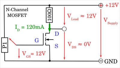
Here, the wiper of the potentiometer is at the upper end, which connects the gate pin directly to the input voltage of +12V. With that, the resistance of the transistor becomes minimal, typically it falls below 1Ω. With that we get for the voltage drop across the drain-source path of the MOSFET: VDS = 12V * 1Ω / (1Ω + 100Ω) = 0.1188V For the voltage drop across the load there is: VLoad = 12V - 0.1188V = 11.8812V More or less the total input voltage now drops across the load resistor, while the voltage across the MOSFET is almost 0V. For the current through the load resistor and thus also into the drain pin, there is: ID = 12V / (1Ω + 100Ω) = 0.1188A The behavior of a depletion type MOSFET differs in that the resistance is minimal at 0V between gate and source (usually less than 1Ω) and it increases to its maximum (about 1MΩ) when the voltage at the gate reaches its maximum, too. How this type of field effect transistors work is written in the chapter about JFETs. The more common type is the enhancement MOSFET, which is why I am treating this type of transistors in this chapter. Threshold voltage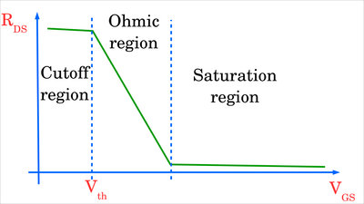
The correlation between resistance of the drain-source path and gate voltage is not linear over the entire range! It is therefore not to be assumed that the drain-source resistance is half the maximum at half the input voltage at the gate pin. The correlation is more complex and a characteristic value to be considered is the so-called threshold voltage (Vth). Put simply, the drain-source resistance is more or less maximum below this threshold voltage; even large variations in the gate voltage (as long as it remains below Vth) cause only a very small variation of the transistor resistance. The range of the gate voltage from 0V to the threshold voltage (Vth) is therefore called cutoff region. In the range up to slightly above Vth, the drain-source resistance changes dramatically even with small variations in the gate voltage and now there is an (almost) linear correlation between gate voltage and resistance of the drain-source path. This small range (usually less than 1V) is therefore referred to as the linear or ohmic region. If the transistor resistance falls close to its minimum while the gate voltage continues to rise, the MOSFET goes into the so-called saturation region. In this region, a further increase in gate voltage causes only a very slight change in drain-source resistance, which is now very low anyway. Amplifying digital signals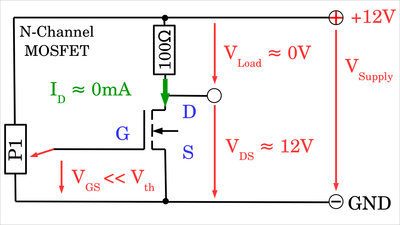
In this chapter I would like to deal with the amplification of digital signals. Put simply, it is about switching a MOSFET ON or OFF, i.e. operating it in such a way that the drain-source resistance is either minimal (the transistor is switched ON) or maximal (the transistor is switched OFF). Let's start with the "turned off" case. As already described above, this is the case whenever the voltage between gate and source is 0V. As long as the gate voltage remains well below the threshold voltage, this condition stays sufficiently fulfilled. In practice, well below Vth means more than 1V away from it. It should be noted that so-called signal noise always occurs in real circuits, i.e. the voltage fluctuates around the specified value. It must be avoided that the gate voltage in the switched-off state plus the maximum voltage caused by noise gets in the range of the threshold voltage! Thus, the gate voltage should be as close to 0V as possible when switched off. 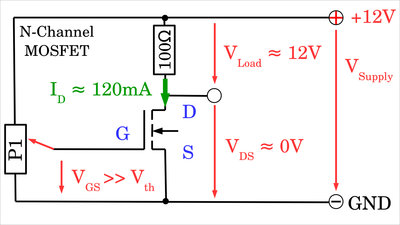
In the ON state, the gate voltage should be kept significantly above the threshold voltage (Vth plus at least 1V). This condition must also take signal noise into account. The higher the gate voltage, the better, but the maximum gate voltage, which is listed in the data sheet, should never be exceeded! Once more, don't forget to consider signal noise, so you should keep a "safety distance" when designing a circuit. Data sheets usually list the gate voltage at which the maximum drain current was measured (e.g. ID = 13A @VGS 10V) or the minimum resistance in the "ON" state (e.g. RDS(on) 50mΩ @ VGS10V). This is the gate voltage to be targeted for the "ON" condition when designing a circuit, at least if you want to go to the limits in terms of power amplification. Switching high output power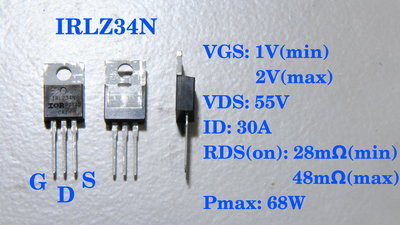
If the signals of the GPIOs of an Arduino Uno or a Raspberry Pi are to be amplified, the MOSFET used must be switched ON clearly at 5V or 3.3V. The threshold voltage Vth must therefore be significantly below the respective control voltage level. In the datasheet of the N-channel MOSFET type IRLZ34N shown here, the threshold voltage is listed between 1.0 (minimum) and 2.0V (maximum) with 1.5V being the typical value. With a gate voltage of 3.3V, the MOSFET can be seen as switched on, but the transistor is only specified for the maximum current with a gate voltage of at least 5V. The maximum drain current is listed with 30A, the maximum drain-source voltage is 55V. 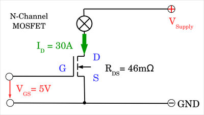
Another important value to be considered is the maximum power the transistor can dissipate. For the IRLZ34N it is listed with 68W. The resistance of the drain-source path is listed between 28mΩ and 46mΩ at a gate voltage of 5V. Let us assume the most unfavorable value of 48mΩ. If the maximum current of 30A now flows through the transistor, the dissipated power is: (1) R = U / I -> U = R * I and (2) P = U * I with (1) you get P = R * I2 = 0.046Ω * 30A * 30A = 41.4W So we are in the "green zone". However, it should be kept in mind that these 41W are transformed into heat that has to be removed from the transistor as quickly as possible. A large heat sink is therefore mandatory! The resistance of 48mΩ is valid at a transistor 25°C and rises with temperature. 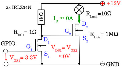
What about a gate voltage of only 3.3V? The IRLZ34N is not specified for this logic level, therefore no data is listed directly. From the diagrams it can be estimated that currents up to 10A can be switched using this gate voltage with good cooling. However, if you want to go beyond this, you can pre-amplify the gate voltage with another transistor: To do this, the drain pin of the first transistor has to be connected to the gate pin of the second transistor and, via a resistor, to the positive input voltage. Now, if 3.3V are applied to the gate of the first transistor, the resistance of the drain-source path of this device drops to less than 1Ω (for the calculation example I assume exactly 1Ω). Transistor 1 forms a voltage divider with the 1kΩ resistor and the following applies to the voltage drop between drain and source: VDS1 = VSupply * RDS1 / (1kΩ + RDS1) = 12V / 1001Ω = 0.012V Those 0.012V are present between gate and source of the second transistor, which is far below the threshold voltage, whereby transistor number 2 is switched OFF; it's resistance is in the range of one megaohm. 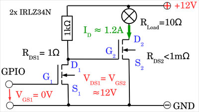
If 0V is applied to the input of the circuit between gate and source of the first transistor, it is turned OFF and the drain-source resistance of the device increases to approximately 1MΩ. With the voltage divider there is for the potential between drain and source: VDS1 = 12V * 1000000Ω / 1001000Ω = 11.988V Now there is a voltage drop of almost 12V between gate and source of the second transistor, which is far above the threshold voltage, so that transistor number 2 is switched ON; it's resistance is now in the range of less than one ohm. The current of the load to be switched flows exclusively via transistor number 2 and with the now significantly increased gate voltage, currents up to the permitted maximum of 30A can be switched. Please note that the signal on the GPIO is inverted! If the GPIO is switched off as shown here, there are 0V at the gate of the first transistor and thus 12V at the gate of the second transistor. This device is switched ON, a current flows through the load. In the previous figure, the GPIO was switched on, resulting in 3.3V at the gate of the first transistor but 0V at the gate of the second transistor. When the GPIO is switched ON, transistor 2 is switched OFF and no current flows through the load. 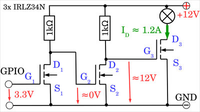
This inverted switching behavior can be corrected by a third transistor: Now, whenever there are 3.3V at the input of the circuit, transistor 1 is switched on, which means that zero volt are present at the gate of transistor 2 and the latter is switched OFF. This in turn means that there is approximately 12V at the gate of transistor 3 and this device is switched on; a current flows through the load whenever the GPIO is switched ON. There is no need to use power MOSFETs for the preamplifying stages. Consider that no more than 12mA flow through transistors 1 and 2, which means that significantly cheaper alternatives can be selected. For many MOSFETs, 5V is also not a sufficiently high gate voltage to switch on reliably! The threshold voltage of the BUZ11 is e.g. between 2.1V (most favorable case) and 4V (worst case), with which the maximum Darain current ID of 30A is only specified at 10V VGS. So when using this MOSFET with 5V logic voltage, a preamplification is also necessary! Be sure to keep an eye on the threshold voltage when purchasing a MOSFET! Maximum gate voltage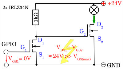
The next point to consider when using preamplifying stages is the maximum gate-source voltage, which is usually lower than the maximum drain-source voltage. For the IRLN34N, VGS(maxx) is 13V, VDS(max) is 55V. If the input voltage of the circuit is increased to 24V, this high supply voltage is present at the gate pin of the second transistor as soon as transistor 1 is turned OFF, which happens whenever the output of the GPIO is 0V. The MOSFET will get destroyed instantly! 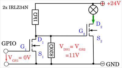
A resistor being connected in parallel to the drain source path of the first transistor is a practical solution. The maximum total resistance of this parallel arrangement of transistor 1 and e.g. an 820Ω resistor is: RTotal = 1MΩ * 820Ω / ( 1MΩ + 820Ω) = 819Ω The resulting voltage at the gate of the second transistor is: VGS2 = 24V * 819Ω / (819Ω + 1000Ω) = 10.8V Which is clearly above Vth and, more important, clearly below the maximum gate voltage. Variable supply voltage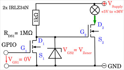
If a variable DC supply voltage is applied to the circuit, a Zener diode can be used to limit the gate voltage at the second transistor. The Zener voltage should be significantly above Vth and below VGS(max). 10V is a good value for the IRLZ34N. If the supply voltage is above the Zener voltage, the gate voltage on the second transistor is limited to the value of this diode. If the supply voltage is lower, VGS2 corresponds (largely) to this input voltage. The minimum voltage this circuit can be operated with is 5V, since, as already discussed, the second transistor won't switch ON cleanly at lower voltages. The maximum supply voltage is now only limited by the maximum drain source voltage of the second transistor. For the IRLZ34N that is 55V. It is important to keep a "safety distance" from VDS(max), since noise must always be taken into account! Flyback diode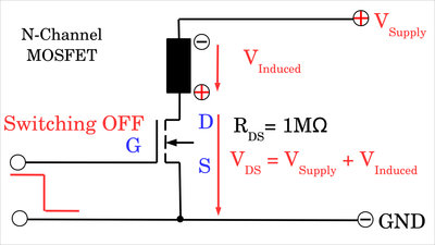
For now I have considered the loads to be ohmic loads. However, relays or motors are often switched via GPIOs. Such inductive loads have a special property: If these are switched on or off quickly, a high voltage that counteracts the external voltage is generated. Whenever an inductive load is switched on, the voltage generated causes the current through the load to rise only slowly. This behavior is not really harmful to a transistors. However, that changes whenever the device is switched OFF: Now, a voltage is induced which tries to maintain the current flow through the windings of the load. This self-induction voltage is added to the supply voltage and is greater, the faster the current flow gets cut off. Since the resistance of the MOSFET rises whenever the device is switched off, all of the supply voltage plus the induced voltage drops more or less across the drain-source path of the transistor. If the MOSFET is operated with a supply voltage being close to the maximum, even a low induced voltage is sufficient to destroy the transistor! 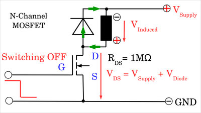
As a protection from high induced voltages, a diode can be connected in parallel to the load in reverse direction with regard to the supply voltage. Now, if an induced voltage builds up in the load whenever the MOSFET is switched OFF, its polarity is in the forward direction with respect to the diode. The current can circle through the load and the diode until the energy stored in the windings is dissipated. During that, no more than the voltage drop across the diode, being operated in forward direction adds up to the supply voltage. A diode operating that way, is named flyback diode. Use a fast switching type with a low voltage drop in forward direction. The reverse voltage should be higher than the supply voltage and the maximum forward current (maximum pulse current) must be able to cope with the current through the load caused by induction. This is usually somewhat higher than the current through the inductive load at full supply voltage. Switching speedSo far we have only considered the two extreme conditions ON and OFF. However, the transition between these two states doesn't appear instantaneous, but takes a certain amount of time. There are usually four parameters listed in the data sheet:
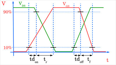
If a load is to be switched very quickly, e.g. while making use of pulse-width modulation for control with variable power, a closer look at the switching times of the transistor is recommended. The time intervals for turn-on delay (tdon), turn-on rise time (tr), turn-off delay (tdoff) and turn-off fall time (tf) are listed in the data sheet. With all four times added up, the worst case scenario for the IRLZ34N is: tdon + tr + tdoff + tf = 21ns + 110ns + 80ns + 65ns = 276ns If one assumes that the transistor should actually be switched on for at least 90% of the periodical time, the resulting minimum is T = 2.76μs and so the maximum frequency is Switching losses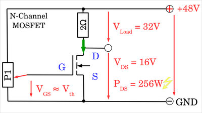
During the switch-on time, the resistance of the drain-source path of a MOSFET changes from approximately one megaohm to less than one ohm. The electrical power to be dissipated by the transistor also varies during this period. The following applies: PDS = VDS * ID = VDS2 / RDS To a good approximation, this power loss is zero while being switched off. For a supply voltage of 12V we get: PDS = 12V * 12V / 1MΩ = 0.144mW We have already seen that the power loss grows to dangerous regions while being switched on. With a high load having a resistance of only 2Ω at a supply voltage of 48V, with a drain-source resistance of 46mΩ (values of the IRLZ34N) we get for being switched on: VDS=VSupply * RDS / (RLoad + RDS) = 48V * 46mΩ / 2.046Ω = 1.02V which is round about 1V For the drain current we get: ID = VSupply / (RLoad + RDS) = 48V / 2.046Ω = 23A and so the dissipated power is: PLoss = VDS * ID = 1V * 23A = 23W That's clearly below the maximum of 68W, However, while the transistor is switched off, the resistance rises to 1Ω in between, by what we get for the current: ID=48V / 3Ω = 16A and so a drain-dource voltage of: VDS = 48V * 1Ω / 3Ω = 16V and finally the power to be dissipated: PLoss = 16V * 16A = 256W Since this excessively high power loss is only reached for an extremely short span of time, the transistor does not blow up immediately. As soon as the switch-off process ends, the power loss drops to almost 0W so that the transistor can cool down again. However, if the transistor is operated with a high switching frequency, the increased power loss during the switching process adds up and can lead to the destruction of the device! Pull-down resistor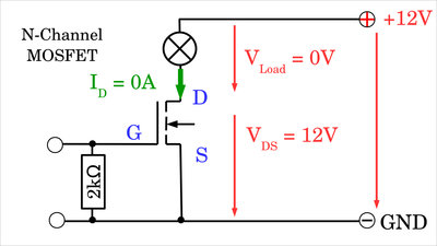
The gate of a MOSFET can be considered to be a very small capacitor. When switching on, a current flows only until the specified gate voltage is reached. In order to maintain this voltage and thus to keep the transistor switched on, (almost) no further electrical power is required. In this state, no (noticeable) current flows through the gate terminal. The current for the IRLZ34N is specified as 1μA. If the gate gets disconnected from the voltage source (i.e. the GPIO), the MOSFET remains in the ON state. If the gate is disconnected when being switched off, the MOSFET remains switched off. Whenever the amplifier circuit is separated from the control voltage, even a tiny charge is sufficient to switch it on. This can happen accidentally by touching the gate terminal with your finger, since the human body usually picks up charges due to the triboelectric effect. To prevent unintentional switching on of a powerful load, a pull-down resistor has to be connected between gate and source of the MOSFET. This ensures that unwanted charge flows out off the gate and the transistor is therefore switched off whenever it is disconnected from the control line. The smaller the resistance of the pull-down resistor, the faster the charge can flow off, but the higher the current flowing when a control voltage is applied. In practice, resistors in the range between 1kΩ and 10kΩ are used. MOSFETs in parallel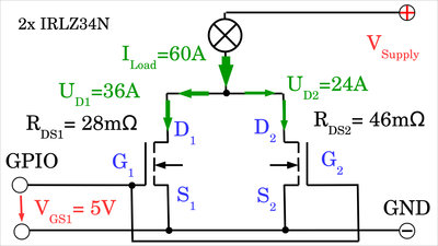
Sometimes MOSFETs are connected in parallel to increase the maximum possible current of an amplifier circuit, but this is not recommended! As already mentioned, the electrical properties of one and the same transistor type varies due to manufacturing tolerances. Let's take the IRLZ34N as an example, again. The turn-on resistance varies between 28mΩ and 46mΩ. Let's now assume the worst case with transistor 1 having the lowest and transistor 2 the highest resistance. The following applies to the current through the two legs of a parallel circuit: I1 = Itotal * Rtotal / R1 or I2 = Itotal * Rtotal / R2 with a total resistance of: Rtotal=RDS1 * RDS2 / (RDS1 + RDS2) = 28mΩ * 46mΩ / (28mΩ + 46mΩ) = 17mΩ When assuming the maximum current of two MOSFETS in parallel is 60A, we get for the current through the two legs: I1 = 60A * 17mΩ / 28mΩ = 36A and I2 = 60A * 17mΩ / 46mΩ = 22A If you add that up, you will see that the total current is only 58A, which is due to rounding errors in my calculation of the total resistance. It is obvious, however, that the current through transistor number 1 is significantly above the permitted maximum! The maximum current cannot be doubled by connecting two MOSFETs in parallel. If a current of 30A flows through the transistor with the lower resistance, the current through the second transistor is: I2 = I2 * R1 / R2 = 30A * 28mΩ / 46mΩ = 18A The maximum total current would be 48A. The current distribution during the switch-on and switch-off process is even more unfavorable, since the time constants are also likely to be different. Parallely connected MOSFETs in commercial applications are devices with very low manufacturing tolerances, usually parts of the same batch, possibly selected according to measured electrical properties. As a hobbyist it is better to look for a MOSFET with a higher maximum drain current. Example circuits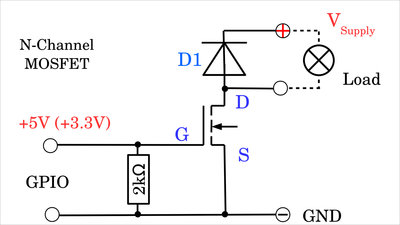
One stage amplifying circuit: Transistor IRLZ34N: With 5V logic level at GPIO, up to 30A, supply voltage from 5V to approximately 36V. Transistor IRF3708: Supply voltage 5V to 20V, at 3.3V logic leve up to 7.5A, at 5V logic level up to 12A. Flyback diode e.g. SR5100, 5A continuous current, 150A peak current, reverse voltage 100V 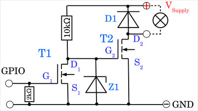
Two stages amplifying circuit (inverted switching behavior): Transistor 1 = BS170 or 2N7000 Transistor 2 = IRLZ34N: Up to 30A, supply voltage 5V to approximately 36V. Flyback diode e.g. SR5100, 5A continuous current, 150A peak current, reverse voltage 100V Zener diode 10V, 500mW 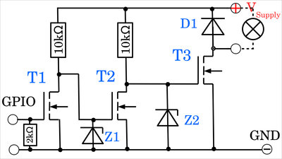
Three stages amplifying circuit: Transistors 1 and 2 = BS170 or 2N7000 Transistor 3 = IRLZ34N: Up to 30A, supply voltage 5V to approximately 36V. Flyback diode e.g. SR5100, 5A continuous current, 150A peak current, reverse voltage 100V Zener diode 10V, 500mW Sourcing partsWhen buying components via the affiliate partner links I have listed in the table (or through the banners on my pages) you help to keep my my projects going - many thanks!Clicking on the links does not mean you have to buy - you can simply browse through the pages ;-) Of course, supporting my freely accessible educational platform without shopping but by making a donation or becoming a Patreon also works. Many thanks to everyone who already sent me an obol! If you know more MOSFETs that are good for amplifying signals of 5V or 3.3V GPIOs or common, cheap power diodes, please leave a comment on this page.
<<< Simple Communication Switching P-channel MOSFETs >>> News The Project Technology RoboSpatium Contribute Subject index Archives Download Responses Games Links Gadgets Contact Imprint |
|
|