|
|
|
|
News The Project Technology RoboSpatium Contribute Subject index Download Responses Games Gadgets Contact <<< Switching N-channel MOSFETs Demop board H-Bridge >>> Switching P-channel MOSFETsThere is no Video about switching MOSFETs available, yet.Leave a comment, if you have ideas of what to show in that video (besides the things already mentioned on this page).OverviewIn this chapter you can read about:
Positive charge carriers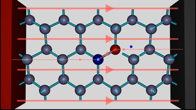
The conductivity of semiconductors based on silicon is achieved by injecting impurities in the crystal lattice. Details can be found in the chapter about doping of semiconductors. In this chapter I will deal with the electrical properties of P-channel MOSFETs, in which the so-called electron holes are the majority charge carriers. These positive charge carriers with a mobility that is significantly lower than that of electrons are quasiparticles. In contrast to N-channel MOSFETs, in which the much more mobile electrons largely transport electrical charges, P-channel MOSFETs are slower in principle. Pin layout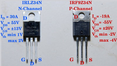
The naming of the pins of a P-channel MOSFET is identical to that of an N-channel MOSFET. Here, too the names are Source, Drain and Gate. An IRLZ34N (N-channel) and an IRF9Z34N (P-channel) MOSFET are shown here. The assignment of the pins of both transistors is identical, but this does not always have to be the case. A look at the data sheet is essential to identify the pins! 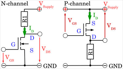
At the latest when connecting a P-channel MOSFET, the differences to an N-channel MOSFET have to be kept in mind: With the P-channel MOSFET, the source pin is connected to the positive supply voltage, while the drain pin is connected to ground via a load resistor. Reminder: With the N-channel MOSFET, the source pin is connected to ground, while the drain pin is connected to the positive supply voltage via the load resistor. In both cases, the potential at the drain pin is somewhere between 0V and the value of the positive supply voltage. The maximum drain-source voltage (VDS) is listed in the data sheet, and in both cases the voltage drop from the drain pin to the source pin is recorded. Since the source pin of an N-channel MOSFET is (usually) at ground, but for P-channel MOSFET at the level of the positive supply voltage, we get a positive reading for VGS at N-channel MOSFETs, but a negative reading at P-channel MOSFETs. 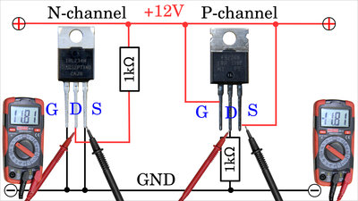
This becomes clear when a multimeter is used for voltage measurement. The red probe is connected to the drain pin of each MOSFET, the black probe to the source pin. It can be seen that when the transistor is switched off (0V across the gate-source path), almost the entire supply voltage of 12V drops across the drain-source path of each MOSFET, but the value at the P-channel MOSFET is displayed with a negative sign. Switching ON and OFF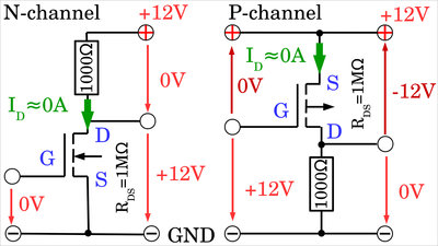
Same as with N-channel MOSFETs, the resistance of the drain-source path changes on changing gate-source voltage. Here too, the resistance for enhancement types is maximum if the potential difference between gate and source is 0V which is the case when the entire supply voltage is present between gate and ground of the P-channel MOSFET. At the N-channel MOSFET to the left there is 0V between gate and ground and between the positive supply voltage and gate pin the entire supply voltage can be measured. Both MOSFETSs are switched off, the resistance of the drain-source path is in the range of one megohm, which means that the total supply voltage drops more or less across the transistors that form a voltage divider with the 1kΩ resistors: VDS = 12V * 1MΩ / (1MΩ + 1kΩ) = 11.99V Again, for the P-channel MOSFET, the reference point of voltage measurement is not the ground, but the +12V cable. Accordingly, the reading on the drain-source path is -12V. 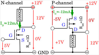
In order to minimize the resistance of a P-channel MOSFET, a negative voltage must be applied between gate and source. Analogous to the N-channel MOSFET, the threshold voltage (VGS) is the voltage value at which the resistance of the drain-source path changes rapidly even with small variations in the gate voltage. The difference is that the voltage of a P-channel MOSFET must be reduced further (meaning "made more negative") in order to reduce the resistance. Same as in the previous chapter about N-channel MOSFETs, let's look at how to amplify digital signals, which means that the gate voltage either corresponds to more or less 0V or should be significantly above (N-channel) or below (P-channel) the threshold voltage. In the worst case, the threshold voltage of the IRF9540 MOSFET is -4V. At a voltage of -5V the transistor can be treated as being switched on, although no high currents (<1A) should be switched with this gate voltage! The drain-source voltage at the N-channel MOSFET is now: VDS = 12V * 1Ω / (1Ω + 1kΩ) = 0.012V ≈ 0V So there is almost no voltage drop across the transistors and the corresponding drain current is: IDrain = 12V / (1Ω + 1000Ω) ≈ 12mA Note that the conventional current (imaginary positive charge carriers flowing from plus to minus) enters the N-channel MOSFET at the drain pin, but leaves the P-channel MOSFET at the drain pin. With that, we get a negative reading for the drain current at a P-channel MOSFET and at the circuit symbol for a P-channel MOSFET, the arrow points away from the transistor, while it points towards the device for an N-channel MOSFET. "uncommon" ground line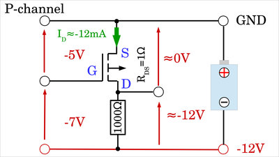
The negative terminal (cathode) of a battery is usually the reference point for voltage measurements (=ground, GND), but for P-channel MOSFETs it is the positive terminal (anode) as shown in this drawing. This once more makes clear why VGS and VDS are listed as negative values in the data sheets of P-channel MOSFETs. 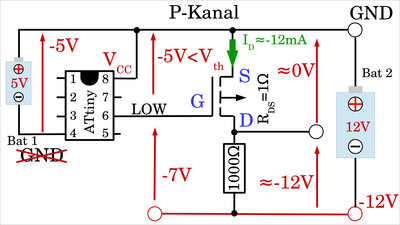
This figure shows how a P-channel MOSFET can be controlled via a microcontroller. A second battery supplies the ATtiny microcontroller with a voltage of 5V. Both batteries are directly joined at their positive terminals which is the reference potential ("ground", GND) in this case. Pin 5 of the ATtiny is labeled GND in the data sheet, so the negative terminal of the battery, which supplies this microcontroller with electrical energy, is connected to this pin. For our overall system, however, this is not ground! Pin 8 is the connection for the positive supply voltage (VCC) of the microcontroller, which is why it is connected to the positive terminal of the battery and so to our reference potential of the overall system (ground). The potential is -5V between pin 4 and our ground wire. Whenever the microcontroller switches a pin to LOW (switched OFF), the potential equals (nearly) that at pin 4, thus we also get a reading of -5V with respect to our ground. The gate-source voltage on the P-channel transistor is more negative than the threshold voltage, the P-channel MOSFET is switched ON at LOW signal on the control pin. 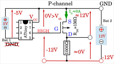
If the microcontroller sets the control pin to HIGH level (the pin is switched ON), the potential equals (almost) the potential at pin 8 (VCC), which corresponds to 0V with respect to our ground (pin 8 is connected to our ground line). Thus, the P-channel MOSFET is switched OFF whenever the control pin is switched ON. Minus is the "better" ground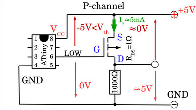
In electrical engineering, the negative terminal of a DC voltage source is usually the ground potential, as is the case in this figure. The circuit works with a supply voltage of +5V and the control pin 6 of the microcontroller is switched off. Thus, there is 0V between pin 6 and ground and -5V between pin 6 and source of the P-channel MOSFET (for the transistor, the source pin is always the reference point). The voltage is below Vth(more negative), which means that the transistor is switched ON whenever the control pin is switched OFF. 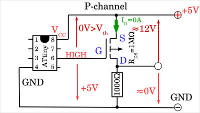
If the control pin is switched ON, there is +5V between the control pin and ground, but 0V between gate and source of the MOSFET. The P-channel MOSFET is switched OFF when the control pin is switched ON. 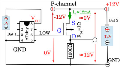
The logic level of the microcontroller is 5V, same as the maximum input voltage of this device. In this drawing, the supply voltage of the output circuit is +12V. If the control pin is switched off, the resulting potential difference to ground is 0V. The voltage between gate and source of the MOSFET is -12V, which is more negative than the threshold voltage, which means that the transistor is switched ON when the control pin is switched OFF, same as in the previous example. 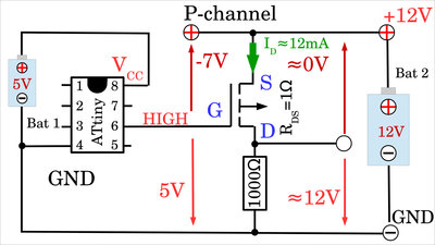
If the control pin is switched ON, there is +5V between pin 6 and ground. Due to the +12V supply voltage at the MOSFET, a potential difference of -7V remains for the voltage between gate and source, which is still more negative than the threshold voltage. The transistor is also switched ON with a HIGH signal at the control pin of the microcontroller. The microcontroller cannot switch OFF the P-channel MOSFET if the supply voltage at the output circuit is significantly above the logic level! Level conversion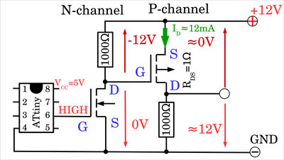
In order to switch a P-channel MOSFET even while being connected to a higher supply voltage, the logic level of the HIGH signal must be raised to the level of this voltage. This is can be done by using a preamplifier stage composed of an N-channel MOSFET: Now, if a HIGH signal is on the control pin, there is +5V between pin 6 and ground, same as between gate and source of the N-channel MOSFET. This transistor is thus switched on and there is (almost) no voltage drop across its drain-source path. As a result, the voltage between gate and source of the P-channel MOSFET is -12V, which is sufficient to also switch that device ON. There is (almost) no voltage drop between drain and source of the P-channel MOSFET and a current of about 12mA flows through the output circuit. Whenever the control pin is switched ON, the P-channel MOSFET is also switched ON. The HIGH level of the microcontroller is converted to the negative value of the supply voltage of the output circuit with respect to the gate-source path of the P-channel MOSFET. 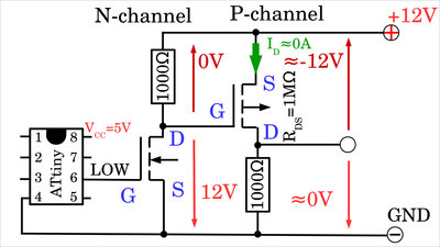
If the control pin is now switched OFF, the voltage drop between pin 6 and ground is (almost) 0V, which also applies to the voltage drop between gate and source of the N-channel MOSFET. This device is switched OFF, so that (almost) the entire supply voltage of +12V drops across its drain-source path. Conversely, the voltage drop between gate and source of the P-channel MOSFET is (almost) 0V. This transistor is therefore also switched OFF and (almost) no current flows through the output circuit. Whenever the control pin is switched OFF, the P-channel MOSFET is also switched OFF. The LOW level of the microcontroller is converted to the value of the supply voltage of the output circuit and thus to 0V with respect to the gate-source path of the P-channel MOSFET. Maximum gate voltage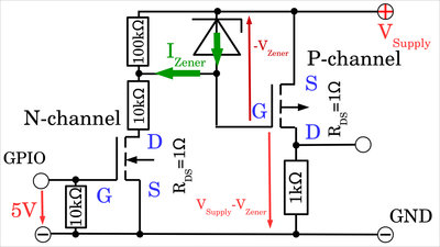
A Zener diode, being connected between gate and source, can be used to protect a P-channel MOSFET from overvoltage at the gate pin. However, an additional resistor is required, which acts as a series resistor, when the N-channel MOSFET of the level converter is switched ON to limit the current trough the Zener diode. Without this series resistor (10kΩ in the drawing), a too high current would flow through the Zener diode as well as the N-channel MOSFET, which would destroy one of the two components! The 100kΩ resistor, the 10kΩ resistor and the drain-source path of the N-channel MOSFET form a voltage divider for which there is: U100k = USupply * 100kΩ / (1Ω + 10kΩ + 100kΩ) ≈ USupply * 0.91 The higher the value of the series resistor, the smaller the voltage drop across the Zener diode. This voltage drop should not fall below the value of the Zener voltage. With a supply voltage of 12V and a Zener voltage of 10V we get: 12V * 0.91 = 10.92V which is in the safety zone. 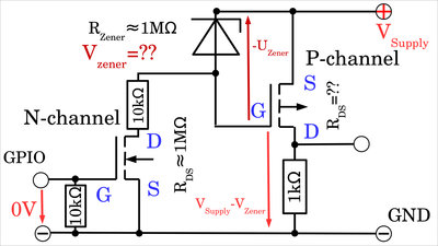
If the 100kΩ resistor in the previous circuit is omitted, as in this drawing, an indefinite situation arises when the level converter is switched OFF: Drain-source path of the N-channel MOSFET, 10kΩ series resistor and Zener diode form a voltage divider. The resistance of a Zener diode below the Zener voltage is in the range of the resistance of a transistor being switched OFF. Thus the gate voltage at the P-channel MOSFET settles somewhere between 0V and the negative Zener voltage by what the transistor is never switched off reliably! 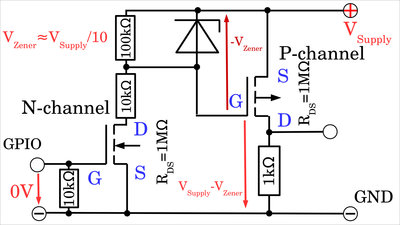
With a resistor connected in parallel to the Zener diode, we get a well defined gate voltage at the P-channel MOSFET when the N-channel MOSFET is switched OFF: UZener = USupply * 100kΩ / (100kΩ + 10kΩ + 1MΩ) ≈ USupply / 10 The smaller the value of the parallel resistor, the more positive (closer to 0V) the gate-source voltage at the P-channel MOSFET when the N-channel MOSFET is switched OFF. This must be significantly more positive (closer to 0V) than the threshold voltage of the P-channel MOSFET. 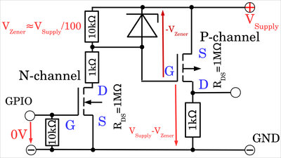
With a high supply voltage, a smaller value is therefore recommended for both, the parallel resistor and the (by a factor of 10) smaller series resistor. With a 10kΩ and a 1kΩ resistor, the resulting gate voltage of the P-channel MOSFET is only one hundredth of the supply voltage when the N-channel MOSFET is switched OFF, which in turn switches OFF the P-channel MOSFET reliably. Note the power dissipation at the series resistor of the Zener diode, that grows with growing supply voltage: P = U2 / R = (USupply - UZener)2 / 1kΩ With an input voltage of 12V we get 0.144W, that grows to 0.576W at 24V. Standard resistors for through-hole assembly are designed for a maximum of 0.25W! Note all extreme values!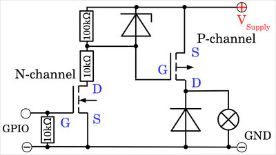
The values for maximum drain-source voltage (VDS), gate-source voltage (VGS) and threshold voltage (Vth), listed in the data sheets, as well as the maximum power dissipation, have to be considered when designing a circuit. Details are available in the chapter about N-channel MOSFETs. To protect the P-channel MOSFET from overvoltage, a flyback diode, being connected between drain and ground with reverse polarity in respect to the supply voltage, should be used when switching inductive loads. A pull-down resistor between gate and source of the N-channel MOSFET is also recommended for safety reasons. Example circuit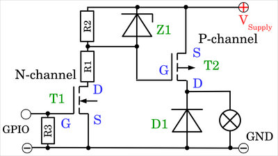
The following components can be used to set up an amplifier circuit for voltages between 12V and 48V at up to 19A (with very good cooling of the P-channel MOSFET): T1 = BS170 N-channel MOSFET T2 = IRF9540 P-channel MOSFET Z1 = Zener diode 10V, 0.5W D1 = Schottky diode z.B. SB5100 R1 = 1kΩ, 3W. At input voltages of less than 15V, 0.25W resistors are good enough. R2, R3 = 10kΩ, 0.25W Sourcing partsWhen buying components via the affiliate partner links I have listed in the table (or through the banners on my pages) you help to keep my my projects going - many thanks!Clicking on the links does not mean you have to buy - you can simply browse through the pages ;-) Of course, supporting my freely accessible educational platform without shopping but by making a donation or becoming a Patreon also works. Many thanks to everyone who already sent me an obol! If you know more MOSFETs that are good for amplifying signals of 5V or 3.3V GPIOs or common, cheap power diodes, please leave a comment on this page.
<<< Switching N-channel MOSFETs Demop board H-Bridge >>> News The Project Technology RoboSpatium Contribute Subject index Archives Download Responses Games Links Gadgets Contact Imprint |
|
|