|
|
|
|
News The Project Technology RoboSpatium Contribute Subject index Download Responses Games Gadgets Contact AmplifierThe video about amplifying circuitsAdjustable resistor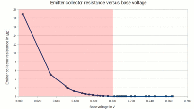
In the chapter about the electrical properties of bipolar junction transistors the above curve progression of the emitter-collector resistance versus base voltage was recorded. The resistance is decreasing from approximately 20MΩ below 1kΩ while the base voltage is increasing from 0.6V to 0.7V. 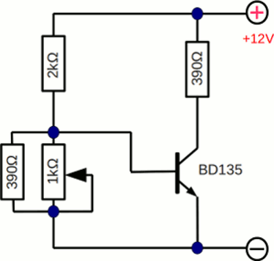
The drawing shows the simplified circuit, used to record the values. The base voltage can be altered by turning a potentiometer and by measuring the voltage drop at the load resistor (390Ω), the resistance of the emitter-collector line was calculated. You might recognize that at the beginning of the series, a huge variation of the base voltage caused almost no variation of the voltage drop at the load resistor or the current running through the base pin. If not, jump back to the chapter, because this is essential for understanding an amplifying circuit. Around a base voltage of 0.6V those behavior changed dramatically. Now a slight variation in the base voltage caused a huge variation in the base current and also in the voltage drop at the load resistor. As you can see at the plot shown above, the resistance of the emitter-collector line is decreasing, hence the voltage drop at the load resistor is increasing. Remember the correlation between total voltage and the voltage drop at a single resistor in a voltage divider: By using Utotal / (R1oad + Rtransistor) = Uload / Rload we get Uload = Rload * Utotal / (R1oad + Rtransistor) The resistance of the load resistor is constant (390Ω), as well as the total voltage (+12V). In contrast, the resistance of the transistors emitter-collector line is varying from 20MΩ to 1kΩ (and less), resulting in a voltage drop from 0.2mV up to 3.4V (and more) at the load resistor. A variation of 0.1V at the base pin caused a variation of 3.3998V at the load resistor. Signal source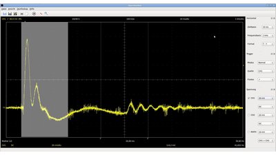
To demonstrate the functionality of amplifying circuits, an input signal is required. I am using a loudspeaker. Normally those devices are used in output mode: An alternating current is running through the wires of an inductor being placed inside of the magnetic field of a permanent magnet. The interaction of the magnetic fields of inductor and permanent magnet results in a force acting on a membrane. Vice versa, if the membrane is actuated, a voltage is induced at the windings of the inductor (see chapter induction). At the drawing you can see an oscillograph curve of a single pulse (tipping with my finger on the membrane) with a peak to peak voltage of approximately 120mV and a pulse length of round about 70ms. Amplifying circuitThe intention is to amplify the signal output of our source - strictly speaking the alternating fraction of the signal. To do so we have to turn the potentiometer until the base voltage is approximately 0.6V. This is the operating point (or bias point) of our amplifying circuit. The resistance of the transistors emitter collector line equals those of the load resistor at the operating point. By increasing the base voltage sightly above the operating point, the voltage drop at the load resistor increases clearly, because of the decreasing resistance of the transistor. On the other hand by decreasing the base voltage slightly, the voltage drop at the load resistor is decreasing significantly, because of the increasing resistance of the transistor.The (alternating) input signal has to be added to respectively subtracted from the (direct) base voltage adjusted at the operating point. There are two ways to achieve this: 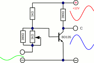
We can open the circuit between potentiometer and ground to switch the loudspeaker in series to the potentiometer. A disadvantage of this principle is the ohmic resistance of the signal source (loudspeaker), which is added to those of the potentiometer. By replacing the signal source by another one with a different ohmic resistance, the operating point has to be readjusted. Another disadvantage is the constant current running through the windings of the inductor even while the membrane is at rest. 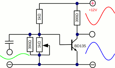
A capacitor is added to the base pin of the transistor. The signal source is attached between the second clamp of the capacitor and ground. Now the capacitor gets charged as soon as a voltage is attached to the circuit. While the membrane of the loudspeaker is not actuated, the voltage drop at the capacitor matches exactly those of the potentiometer, which is the operating point. By tipping on the membrane, the voltage induced by the inductor is added to those of the capacitor. We don't need to readjust the operating point if the signal source is replaced by another one with a different ohmic resistance. The loop running through the base pin of the transistor is called input circuit or simply input. The loop running through the emitter (=voltage between ground and emitter respectively between emitter and positive terminal) is called output circuit or simply output. Accordingly the voltage attached to the input circuit is called input signal, while those recorded at the output circuit is called output signal. Curve progressionThe following curve progressions were recorded by an oscilloscope. The amplifying circuit was attached to a battery with a voltage output of 12V, hence the operating point as to be adjusted in such a way, that the voltage drop at the load resistor equals those at the emitter collector line of the transistor, which is 6V. The accordant base voltage is approximately 0.65V. The used time base was 2ms per division.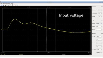
Voltage recorded at the clamps of the loudspeaker: The voltage adjustment is 100mV per division, the zero volt level is at the middle of the display. The measured peak to peak voltage is approximately 250mV. 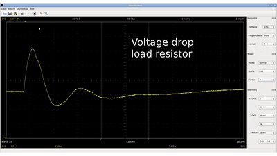
Voltage recorded at the load resistor: The voltage adjustment is 2V per division, the zero volt level is at the bottom of the display. The measured peak to peak voltage is approximately 8V. 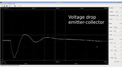
Voltage recorded at the emitter-collector line of the transistor: The adjustments are identical to those of the previous measurement, the peak to peak voltage is similar. The curve progression differs from the plot above. In contrast to the curves recorded at the loudspeaker and the load resistor, the signal starts with a falling slope. This is called phase inversion. Besides the mirror inverted progression of the curve in comparison to those at the load resistor, you might have noted other distortions while looking at the curve progression recorded at the loudspeaker. Distortions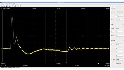
The plotted curve progression of the input signal at the amplifying circuit is different from those recorded without being attached to the circuit (click at the pictures to see the whole plot). Striking are the missing needle shaped peaks in comparison to the original plot. This is caused by the capacitance of the input circuit; remember the capacitor switched in series to the signal source. The electric power of the signal source is low (that's why we are trying to amplify the signal) and some of the power is required to charge the capacitor, which is why the peaks of fast changing input signals are lessened by the device. 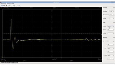
So why don't we simply use a capacitor with a very low capacitance? Because that would reduce the base current running through the transistor, too! The upper plot of the output signal was recorded using a 4.7μF capacitor... 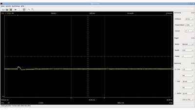
...and the lower one by using a 0.33μF capacitor. You remember the correlation between base current versus base voltage (see chapter properties of bipolar junction transistors)? When increasing the base voltage, the current was increasing, too. Vice versa: to be able to increase the base voltage, the current running through the base pin has to be increased, too. The product of voltage and current is the electric power of a circuit ( Darlington transistor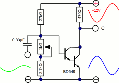
The current gain of power transistors is approximately 10. If a high output power is required, the input signal must provide a current which is just 10 times lower than those of the output signal. If your input signal doesn't provide such a high current, you can amplify the input signal by using a small signal transistor and using the output of the first amplifying circuit as input of the second circuit with the power transistor. Instead of two entire circuits, you can use two bipolar transistors connected in such a way that the current amplified by the first transistor is amplified further by the second one. A compound structure using this principle is called Darlington transistor. The bias voltage at the operating point is approximately twice the voltage of a normal transistor, because there are two junctions between base and emitter of the Darlington transistor. Output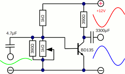
The amplifying circuit has boosted the peak to peak voltage of the input signal from just 0.25V to 8V. But what about the output power? If you would connect another loudspeaker at the output clamps of the amplifier, you won't hear anything coming out of it while tipping at the membrane of the loudspeaker connected to the input circuit. When checking the output voltage of the circuit, you will recognize that there is a clear shift of the operating point! Consider the very low DC resistance (normally 4Ω or 8Ω) of the loudspeaker, which is now connected in parallel to the load resistor (390Ω). Turn on your brain before readjusting the operating point!. The voltage drop at the load resistor is 6V at the operating point, hence the current running through the device is A simple solution to that problem is connecting a capacitor in series to the output circuit. Now the direct current fraction is locked from running through the output circuit. As soon as the voltage drop at the load resistor alters (caused by an altering input signal), a current is running through the output loudspeaker. The power output of the circuit is still very low, hence just a low sound is coming out of the device. Remember the maximum direct current running through the load transistor is Push-pull output circuit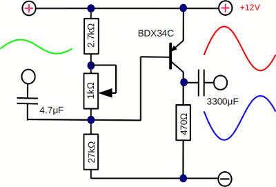
When using a PNP transistor instead of a NPN transistor, the circuit has to be altered slightly. Now the resistance of the transistor (hence the voltage drop) is increasing with increasing (positive) input voltage. The load resistor is connected between ground (negative terminal) and collector. 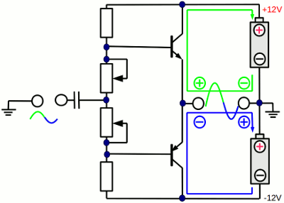
A push-pull amplifier consists of two transistors, one being a NPN type and one being a PNP type receiving the same input signal. Those transistor pair is typically matched in specifications except for polarity. Matched inverted polarity devices are called complementary pairs. The circuit is connected to two independent voltage sources (e. g. two batteries with an output voltage of 12V). The positive terminal of the lower battery is connected to the negative terminal of the upper battery. This point is the reference potential (ground). The upper, NPN transistor becomes conductive if a positive voltage is applied between ground and input clamp. Now electrons can run from ground via the output loudspeaker and the NPN transistor to the positive terminal of the upper battery. The negative terminal is at the right side of the output clamps (the electrons are pushed from the right to the left through the loudspeaker). When applying a negative voltage to the input clamp, the lower, PNP transistor becomes conductive, hence electrons are running from the negative terminal of the lower battery via the PNP transistor and the loudspeaker to the ground clamp. Now the positive terminal is at the right side of the output clamps (the electrons are pulled from the left to the right through the loudspeaker). 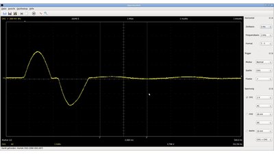
Without a bias voltage attached to the base pins of the transistors, crossover distortions can be detected at the output curve. Remember that the resistance of a transistor is almost not varying at base voltages between 0.0V and 0.6V (NPN), respectively 0.0V and -0.6V (PNP). Hence a variation of the input voltage between -0.6V and +0.6V causes no voltage drop at the output clamps. To eliminate those distortions, a bias voltage has to be applied to the base pins of the two transistors. This can be done by using constant or adjustable resistors (potentiometer) or by forward biased diodes. Attaching the bias voltage to the base pins causes another effect: The resistance of both transistors decreases, hence a higher current is running from the positive to the negative terminal through the emitter collector lines of the devices. Those current is running even without attaching a voltage to the input clamp. 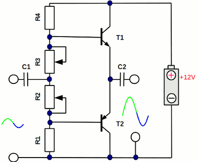
For the recording of the crossover distortion I have used a more simple circuit with only one voltage source: R1=R4=27kΩ R2=R3=1kΩ Potentiometer with 2kΩ resistor in series. C1=0.33μF C2=3300μF T1=BD649 T2=BDX34C Non linear amplifyingThe measure of the ability of an amplifier to increase the power or amplitude of a signal from the input to the output is called gain. Let's have a closer look at the gain of an amplifying circuit used above: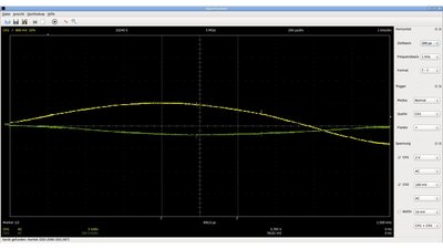
Peak value of the input signal (green line) = 0.4Div Peak value of the output signal (yellow line) = 1.0Div 
Peak value of the input signal (green line) = 0.8Div Peak value of the output signal (yellow line) = 1.5Div. Assuming the gain of the upper plot, the expected value would have been 2.0Div. The gain is clearly lower at higher input values. The correlation between input and output voltage is not linear. 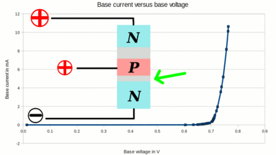
The non linear amplifying is caused by the non linear (no straight line) correlation between base current and base voltage (see chapter electrical properties of bipolar junction transistors for details). Clipping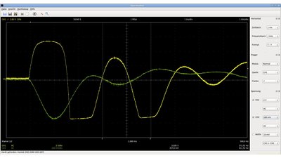
The output voltage of an amplifier can't exceed the voltage of the power supply. If the amplifying circuit is pushed to create a signal with a higher voltage than it's maximum capability, the output signal is cut or clipped at those maximum value. The result is a sine wave becoming a distorted square-wave-type. ConclusionIdeally an amplifier increases the power of a signal without otherwise altering it. As we could see, the input signal is always affected by the amplifying circuit. Only some of the effects were mentioned at this chapter. Depending on the quality of the amplifying circuit, distortions can be limited, but never wiped out completely. Random fluctuation in an electrical signal is a characteristic of all electronic circuits. Those random fluctuation is called noise. Practical amplifiers have finite distortion and noise which they invariably add to the signal.News The Project Technology RoboSpatium Contribute Subject index Archives Download Responses Games Links Gadgets Contact Imprint |
|
|